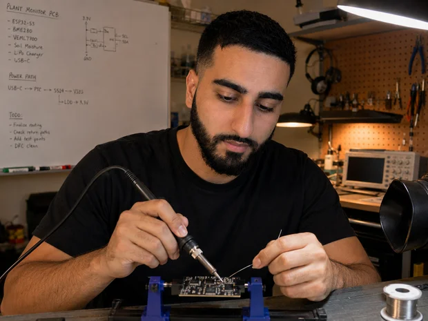
Ray Malik at his electronics bench — oscilloscope, finished boards and a KiCad layout on the screen behind him
Ray Malik hand-soldering a circuit board held in a PCB holder at his bench

Ray Malik

PCB design engineer · MuffinByteLabs

I turn circuit ideas and breadboard prototypes into boards a factory can actually build — schematic, layout, and the complete manufacturing package. Computer-science degree underneath, so the layout is drawn knowing what the firmware will ask of it.

  • Fixed quote in 24hscope, price and timeline in writing
  • Money-back guaranteein every signed contract
  • You own every filenative KiCad, no conversions

Work

PCB 1Built · bring-up passed

ESP32-S3 Wi-Fi Plant Monitor

A battery-powered Wi-Fi sensor node: temperature, humidity, pressure, light and soil moisture, on four layers with a proper ground plane pair.

esp32s3-plant-monitor
  • 62.5 × 44.5 mm
  • 4-layer
  • ESP32-S3
  • USB-C + LiPo
3D model
Layer
Q3R16C10BOOTC8U5C1D1R14C7R11ANT KEEP-OUTU3R5C14U1J2R10R3C3RESETC13C11R1C4R2R7U6C5R9C17F1C9J1U4C12C15R12Q1R4R13J3C2D4R8U2C6R6C18C16Q2R15USBESP32-S3+-SIGPWRCHGPWRBATSOILBME280VEML7700B.SILK — ESP32-S3 PLANT MONITOR · REV A · 2026-08 · MuffinByteLabs.comBAT_SNSIO0TXRXGNDSOIL_ADCENVSYSGND5VVBAT3V3
Trace a net

Pick a net to light it through the copper.

Stackup
4-layer1.6 mm FR-4
  • F.MaskSoldermask
  • F.CuSignal + pours1 oz
  • Prepreg76280.21 mm
  • In1.CuSolid ground, no signals0.5 oz
  • CoreFR-41.06 mm
  • In2.CuSolid ground, no signals0.5 oz
  • Prepreg76280.21 mm
  • B.CuSignal + pours1 oz
  • B.MaskSoldermask + ID block
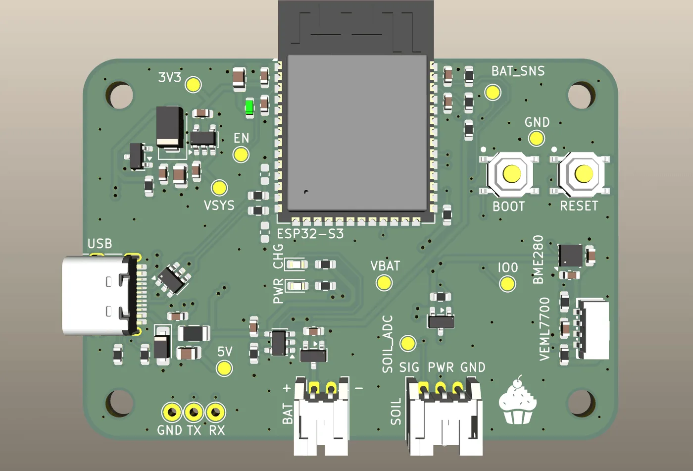
KiCad 3D view of PCB 1 fully populated, seen from above: the ESP32-S3 module with its antenna overhanging the top edge, USB-C on the left edge, BOOT and RESET buttons, BME280 and VEML7700 sensors on the right, and battery and soil connectors along the bottomPopulated
Every part placed and checked for fit before a single board was ordered.
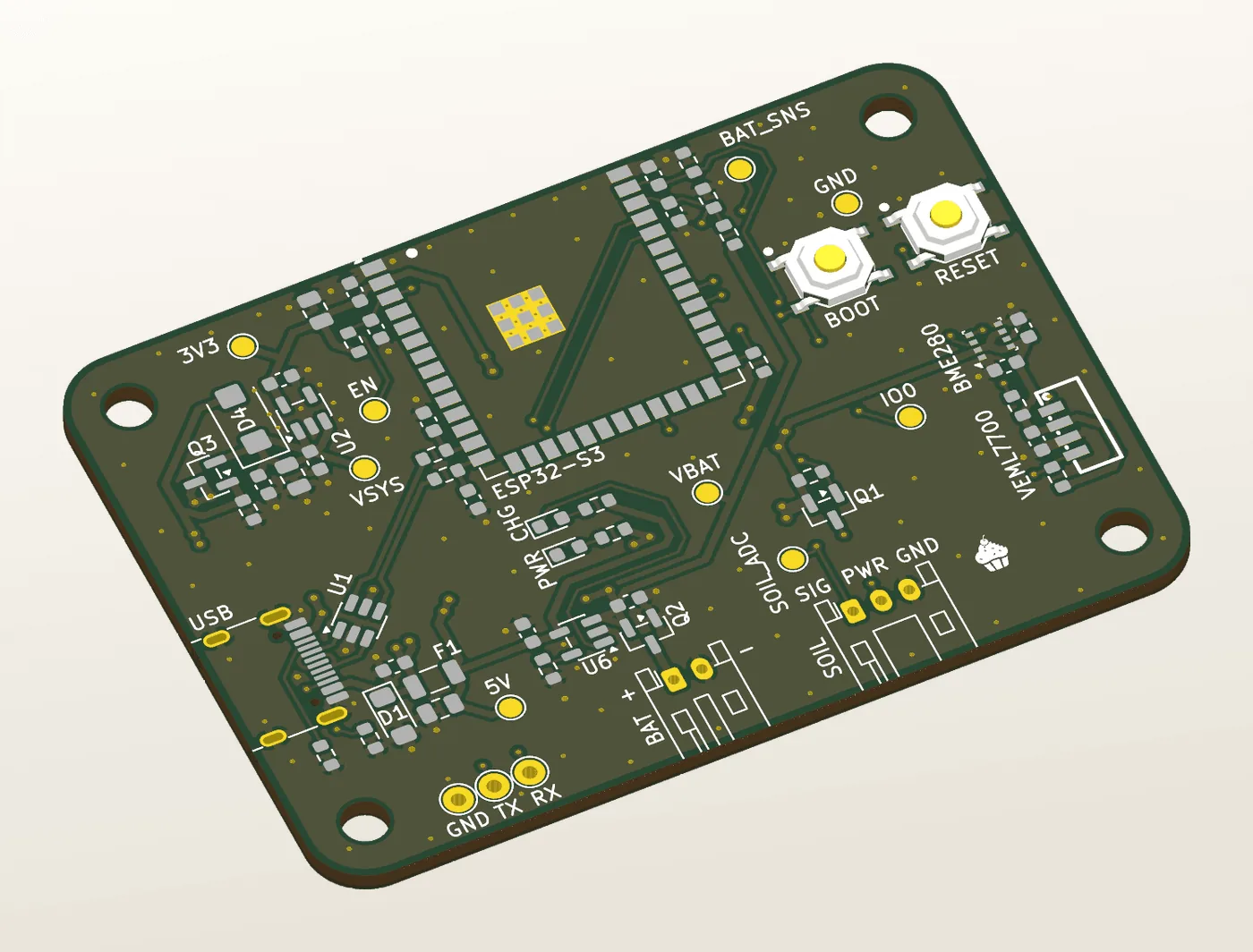
Angled KiCad 3D view of the bare PCB 1 board showing the routed copper, the module's exposed ground pad with its stitching vias, twelve gold test points and four M3 mounting holesBare board
The same board stripped back to bare copper, test points and mounting holes.
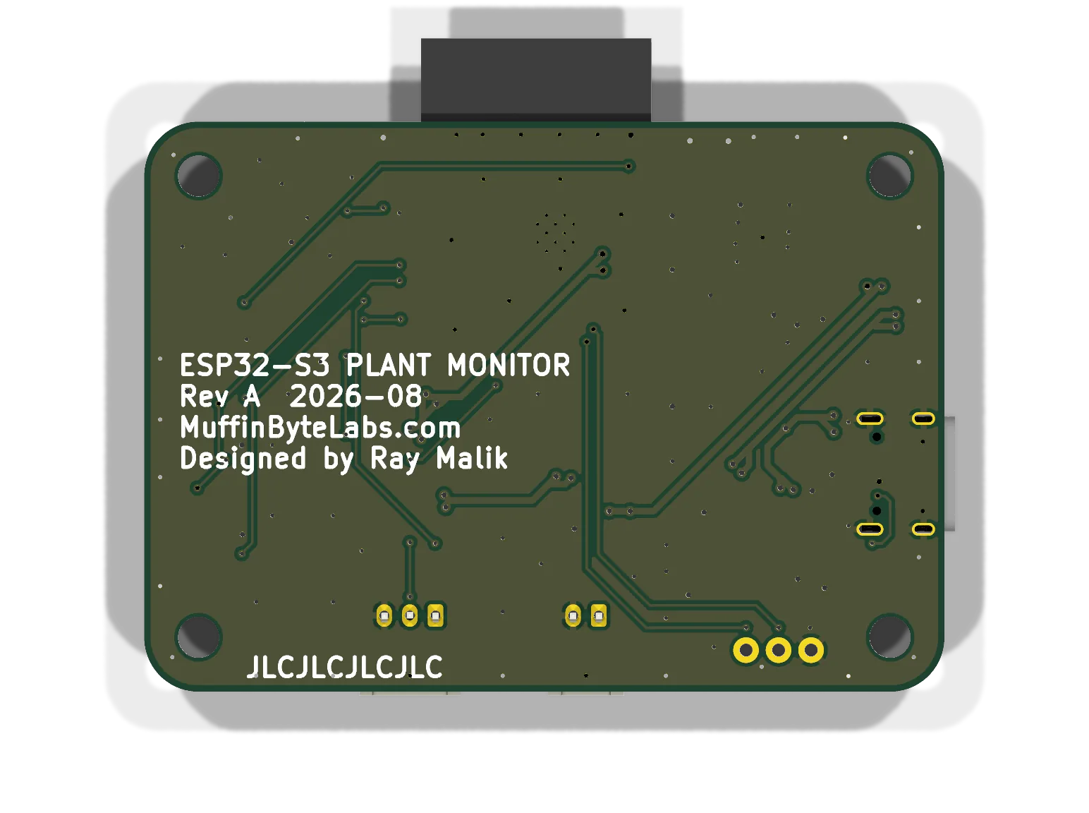
KiCad 3D view of the PCB 1 bottom side: light routing over the plane pair, the through-hole UART recovery pads, and a silkscreen ID block reading ESP32-S3 Plant Monitor, Rev A 2026-08, MuffinByteLabs.com, designed by Ray MalikBottom
The back side, with the ID block every board ships with — name, revision, date, and who to ask.
PCB 2Ordered · in fabrication

Protected Field I/O Controller

A Wi-Fi board that safely reads 24 V equipment signals and switches real equipment — opto-isolated inputs, relay and MOSFET outputs, behind a proper isolation barrier.

  • 110 × 76 mm
  • 2-layer
  • ESP32-S3
  • 9–36 VDC / 24 VAC
Layer
ANT KEEP-OUTU1ESP32-S3-WROOM-1J1U3R1R2R3R4C7C8U4L1C9R5R6R7R8U2C1C2U5U6U7U8R18R19D11IN1R20R21D12IN2R22R23D13IN3R24R25D14IN4K1SPDT · 2 A @ 30 VCOILNO·C·NCK2SPDT · 2 A @ 30 VCOILNO·C·NCQ1Q2R13R14R15R16D9D10RLY1RLY2Q3Q4R9R10R11R12D7D8JP1VLOADJ3J224V INJ4J5J7PUMP+ · P2+ · VLOADF1~ ~+BR1D15+C10PCB 2 · FIELD I/O≤ 2 A @ ≤ 30 V — NOT FOR MAINSLOADS SHARE GND · NOT ISOLATEDVALVEAUXIN1–IN4 · COM9–36 VDC / 24 VACB.SILK ID — MuffinByteLabs · REV A · QRLOGIC SIDEFIELD SIDEVIN5V3V3GNDGNDSWENIO0TXRXGND
Trace a net

Pick a net to light it through the copper.

Stackup
2-layer1.6 mm FR-4
  • F.MaskSoldermask
  • F.CuSignal + field power1 oz
  • CoreFR-41.53 mm
  • B.CuUnbroken ground return1 oz
  • B.MaskSoldermask + ID block
Open source

The whole board, in public

You do not have to take any of the above on trust. PCB 1 is published in full — the KiCad project, the exact package that was uploaded to JLCPCB, the written design document, and the review records that caught two real problems before boards were built with them. Read the work before you hire the person who did it.

MuffinByteLabs/esp32s3-plant-monitor
View the repository
  • hardware/

    The KiCad 10 project itself — hierarchical schematic, 4-layer board, and the footprint and symbol libraries it depends on. Open it and edit it; nothing is locked.

  • fabrication/

    The frozen manufacturing package, exactly as uploaded: Gerbers, drill, BOM and CPL for the revision that was ordered. Not regenerated for the repo — archived at order time.

  • docs/

    The written design document, the bring-up guide, engineering notes and layout rules. Every part on the board has a paragraph saying why it is there.

  • references/

    Every datasheet and reference design the choices were made from, so a reviewer can check the arithmetic without going hunting.

  • firmware/

    Not written yet — a README stating the duties the hardware hands to the firmware: no Wi-Fi transmit below 3.5 V, deep sleep at 3.0 V, and the soil-probe timing. The layout was done knowing them.

Read it in the browser

No KiCad install, no download — each opens as a page and takes about ten seconds to judge. The first two are the reviews this board passed through before it was ordered; a review from me arrives in the same shape — findings, severities, and what to do about each.

Also in there

  • Five review recordspre-fab, placement, finishing and final layout — findings, severities, fixes
  • A footprint check recordevery footprint verified against its land pattern before ordering
  • The pre-order gate listDRC / ERC clean, schematic parity, polarity checked against a pin-1 table
  • A bring-up guidestaged, with the number each step has to hit
  • Rev B notesan honest list of what I would change next

Published under CERN-OHL-P v2 — a permissive open-hardware licence, so you may read it, build it, or lift a block out of it for your own board. It is also a fair sample of what your project would look like when I hand it over.

Capability

Anyone can route a board that looks finished. Below is what sits underneath one — the circuit blocks I design, the layout rules I hold to, and the manufacturing decisions taken long before a file leaves.

  • CAP-01

    Schematic & circuit design

    A schematic is a document before it is a netlist. If a reviewer cannot follow the circuit without opening the board file, it is not finished.

  • CAP-02

    Power & protection

    Every rail gets a written worst case before a part is chosen, and every input is designed on the assumption that the supply will one day arrive backwards.

  • CAP-03

    Field interface & isolation

    The optocouplers and the relay contacts break the path between your equipment and this board. The copper around them is a separate return — drawn as a distance, defended on every layer, bonded at one deliberate point. Naming which of the two is doing the work is the job.

  • CAP-04

    PCB layout

    On four layers the return current has a path directly under the trace that carried it. On two, the pour has to be kept whole enough to give it one. Either way the board is quiet by construction, not by luck.

  • CAP-05

    Manufacture & bring-up

    A board is not finished when it routes. It is finished when someone who has never spoken to me can order it, build it, and prove it works.

Every board ships with

  • GerbersRS-274X, one file per layer
  • Drill filesExcellon, plated and non-plated
  • BOMreal manufacturer part numbers, stock checked
  • CPL / centroidX / Y / rotation per part
  • Schematic PDFreviewable without opening KiCad
  • Paste + stencil notesapertures checked against the datasheets
  • DRC + ERC proofzero errors, screenshots included
  • README + REV notesthe design intent, and what changes next
  • Native KiCad sourceyou own the project, not just the artwork

Quoted both ways, every time: turnkey assembly and bare-PCB-plus-stencil are different economics, and the crossover moves with quantity, part count and schedule. Running that comparison against your actual numbers is the part a fab's instant-quote page cannot do for you.

Start a boardFixed quote in 24 hours — scope, price and timeline in writing.